$11.75
Add to Cart
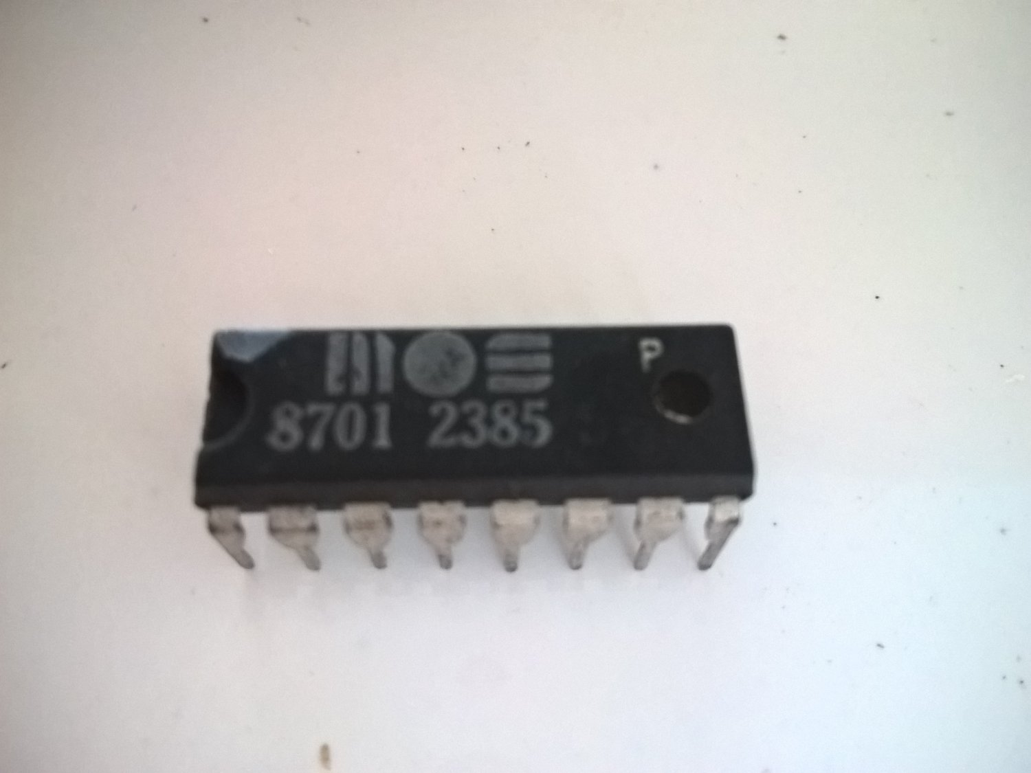
MOS 8701 Chip, NEW OLD STOCK, C64 Clock Generator, Commodore CBM 8701-1


Appearance: New, slight wear
Functionality: New
Description:
============
Similar to pictured, a Commodore 8701 chip – new old stock. Includes just the bare chip.
Warranty and Returns:
=====================
We understand that there may be compatibility issues, space constraints, or it just doesn’t look perfect. This item can be returned within 14-days for ANY reason. However, shipping to and from is not refundable.
Shipping:
=========
- Other shipping methods are available – contact us for details.
- Combined shipping is available for most items – contact us for details.
- Local pickup is also available at no cost.
About Us:
=========
The Computer Preservation Group is dedicated to the preservation of historical computers. To help fund ongoing operations, select items are made available. To learn more, please visit our website: www.computerpreservation.com. Thank you for your support!
Stock#:C6516.EG#.1
Details from ftp://www.zimmers.net/pub/cbm/documents/chipdata/8701.txt:
The pinout of the clock chip obtained from the schematics is as follows:
1 16
GND 2 15 +5V
3 14 Crystal In
GND 4 13 Crystal Out
5 12 +5V
Dot Clock 6 11
Enable PAL 7 10
Color Clock 8 9 GND
N/C 1 16 N/C
VSS 2 15 VCC
N/C 3 14 Crystal In
N/C 4 13 Crystal Out
-Reset 5 12 VCC
Dot Clock 6 11 N/C
Enable PAL 7 10 N/C
Color Clock 8 9 VSS
Note the differences on pins 4 and 5.
My experiments on the chip reveal the following, which are not entirely
consistent with the Commodore specifications:
1. If you disconnect pin 12, the entire chip is dead. If you disconnect
pin 15, the crystal stops oscillating and all outputs stay at a constant
level, but the chip is not dead. Therefore, pin 12 is the true Vcc and
pin 15 is the +5V level for the crystal.
2. If you disconnect pin 9, all functions on the chip stop. If you
disconnect pin 2, the outputs stop, but the crystal still oscillates. If
you disconnect pin 4, an output appears on pin 11. Therefore, pin 9 is the
true Vss, pin 2 is the output enable, and pin 4 is the enable for pin 11.
3. If you ground pin 5 (-Reset), the dot clock stops, but not the crystal.
4. Pin 10 maintains a constant output at +5V.
5. I have found no functions for pins 1, 3 and 16.
If you incorporate all this information into a pinout, it would look like
the following:
N/C 1 16 N/C
Output Enable 2 15 +5V for Crystal
N/C 3 14 Crystal In
Disable pin 11 4 13 Crystal Out
- Reset 5 12 Vcc
Dot Clock 6 11 Unknown Output
Enable PAL 7 10 +5V Constant Output
Color Clock 8 9 Vss
Enable or disable is accomplished by tying to ground.

